
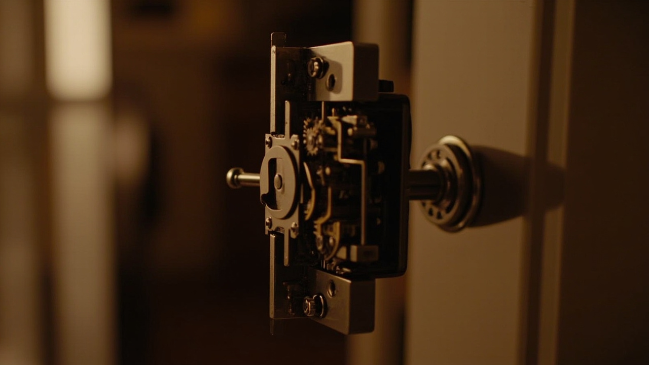
How PCB Layout and Protection Drives Smart Lock Reliability
Most system integrators meet the control board late: after the door schedule, power assumptions and credential plan are settled. The board sits behind the keypad, fingerprint sensor, RFID/IC card reader, battery compartment, motor and gearbox, or latch drive. Yet every command, reading and event record crosses its copper. The pcb layout and protection reliability link is not a line in a catalogue; it is the sequence that decides whether electrical stress is contained near its source or allowed to become a reset, a false state or an intermittent lock.
Direct answer. The short answer is that pcb layout and protection reliability link is not one decision. It is a sequence. This article takes pcb layout and protection reliability link from pcb layout and protection reliability link through pcb-layout-and-protection to the record you keep. A pcb layout and protection reliability link is a component-level look at how the technology behaves. pcb layout and protection reliability link is where the limits sit. pcb layout and protection reliability link is verified on the dated product page.
pcb layout and protection reliability link is used here in the sense given under pcb layout and protection reliability link. It is a working definition of pcb layout and protection reliability link that carries no regulatory weight. The buyer still has to check it against the dated product page.
- Verify the function — confirm on the dated product page for the specific SKU behind pcb layout and protection reliability link
- Verify the boundary — record where the technology in pcb-layout-and-protection stops working
- Verify the backup — name the mechanical path that remains if pcb layout and protection reliability link fails
- For pcb layout and protection reliability link, pcb layout and protection is what each step has to answer to.
The qualification bench turns a board into a system
The first-party catalogue contains 79 published models, but reliability cannot be inferred from model count. It has to be traced through the hardware that carries power and signals. The published first-party record for the SLK-9936S hotel lock, for example, lists RFID/IC card capability, four AA cells, a 3-point latch and a 36–100 mm applicable door thickness. Those figures place the board inside a real mechanical and power envelope; confirm on the dated product page for the specific SKU before using any of them in a procurement decision. If the answer has to survive a supplier meeting, PCB Layout and Protection in High-Traffic and Harsh Environments is the next one to read.
Start qualification at the opening rather than the enclosure. Door thickness, backset, panel space, power source and credential interface constrain what the control PCB can become. The Office Smart Lock Site Survey and Smart Lock Retrofit Site Survey establish this door-first sequence. Once those boundaries are known, the board can be reviewed as part of the lock rather than as an isolated electronic deliverable.
The path hidden behind the panel
Follow one credential event through the product. A reading enters an interface, crosses protected wiring, reaches a processing section, and produces a command for the motor, latch or bolt drive. Each transition offers a place where an interruption can become a field symptom.
flowchart TD
    A["Stress enters a connector or power input"] --> B["Protection stage responds"]
    B --> C["Layout routes energy and signals"]
    C --> D["Control state stays predictable"]
    D --> E["Access operation remains available"]
    B --> F["Stress reaches a sensitive circuit"]
    F --> G["Noise, heating or reset"]
    G --> H["Field failure and service call"]
This sequence is more useful than a single reliability claim. It tells the integrator where to inspect, which evidence belongs to which transition and whether a symptom is more consistent with a power disturbance, a routing issue or an external mechanical event.
Geometry decides how much work protection must do
Control PCB layout is an energy-routing decision. Power-conversion components, protection devices, processing circuitry, motor control and sensitive interfaces each have different current, voltage and switching conditions. Their placement determines how quickly an disturbance is redirected and how well a useful signal returns to its intended circuit.
A protection component cannot compensate for every poor layout choice. If the route from a connector to the protection stage is long, or its return path passes beside a motor-drive section, the protected circuit may already have been exposed before the protection device acts. Decoupling, return-path continuity and separation of sensitive routes therefore belong in the same review as component selection. This is the pcb layout and protection reliability link in practical terms: geometry determines the stress presented to protection, while protection limits the consequence of that geometry.
Protection works as a chain
Ask what response is required at each energy entry point. For battery input, request evidence of reverse polarity protection and defined overvoltage behaviour. At an exposed interface, ask how ESD protection is arranged and where its return terminates. For an externally connected line, request the surge protection approach and its relationship to the connector.
| Disturbance or input | Protection question | Layout evidence to request | Qualification observation |
|---|---|---|---|
| Reversed battery input | Is reverse polarity protection present? | Blocking element and return path near the input | Behaviour under the agreed reversed-input procedure |
| Electrostatic discharge at an interface | How is ESD protection arranged? | Placement, routing and defined return | Response under the agreed electrostatic procedure |
| Transient on an external line | What surge protection approach is used? | Protection at the entry point and a short return path | Behaviour at the interface and downstream |
| Motor or latch-drive activity | How is switching noise separated? | Distance, return routing and interface filtering | Control response during repeated operating cycles |
These are questions and test objectives, not claims about a particular supplied board. Placement often reveals more than a parts list. A long unprotected approach to a connector, an ambiguous return or a dense interface between motor drive and credential circuitry can weaken an otherwise reasonable protection concept.
A symptom can point backward through the chain
Field symptoms become more useful when the investigation starts with isolation rather than replacement. Record the power condition, operating mode, door movement and recent environmental event before changing hardware. Then move backward through the diagram, separating the external system from the protected board and the protected board from the component that appears to have failed.
| Field observation | First isolation step | Evidence to request | What the observation alone cannot prove |
|---|---|---|---|
| Intermittent unlock command | Separate manual operation from electronic control | Board power record, signal path and motor-drive layout | Which individual component failed |
| Reset during lock movement | Check power interruption and motor activity | Input protection, return paths and operating-cycle procedure | Whether protection or layout caused the event |
| Irregular low-battery alert | Verify cell condition and measurement point | Battery monitoring section and relevant layout | Whether the alert circuitry is defective |
| Variable reader response | Separate credential events from motor activity | Interface routing, return arrangement and module boundary | Whether the credential itself caused the variation |
The PCB Layout and Protection Failure Modes Seen on Smart Lock Projects provides a broader symptom-based structure. The board should be evaluated as one link in that chain, not treated as the automatic cause of every electronic symptom.
An illustrative qualification from door to evidence
Consider an illustrative qualification in which a system integrator is comparing a lock for repeated daily use. No failure has yet occurred. The first task is to document the opening, power arrangement, expected operating cycles and the interfaces that must remain available. That baseline prevents later test observations from being interpreted without context.
The integrator then reviews the schematic and layout, identifies every external entry point and checks the placement of protection. Sample units then follow an agreed procedure covering reversed input, defined transient exposure, electrostatic discharge, repeated motor operation and the specified operating environment. Every observation is tied to the exact board revision and enclosure configuration. The outcome is not a generic statement about smart lock reliability; it is a traceable record showing which stresses were introduced, how the product responded and what remains unverified.
The PCB Layout and Protection Test Evidence a Buyer Can Actually Request helps separate a usable procedure from an impressive but ambiguous test description. The evidence should identify the sample, revision, setup, observation and acceptance condition.
The comparison belongs in the purchasing record
Several board strategies may meet the same access function. The buyer should not award preference merely because one strategy sounds more integrated or more serviceable. The useful comparison is where containment, diagnosis and manufacturing consequences sit.
| Buyer decision | Possible route A | Possible route B | Comparison evidence | Practical consequence |
|---|---|---|---|---|
| Board partitioning | Integrated control section | Separated power, motor and sensing sections | Schematic blocks, layout and assembly plan | Compare fault containment and inspection scope |
| Protection placement | Concentration at the entry point | Layered protection near vulnerable circuits | Component placement and return routing | Compare the stress path before the sensitive circuit |
| Service access | No dedicated programming or test access | Defined test or programming points | Dated drawing and service procedure | Compare diagnosis effort after installation |
| Environmental grouping | Mixed placement by component type | Grouping by exposure and function | Assembly and inspection plan | Compare repeatability of environmental review |
These are architectural choices, not descriptions of supplied SKUs. A written comparison prevents an assumption from becoming a specification. The Specifying PCB Layout and Protection: Questions that Get Real Engineering Answers provides a structured way to identify which route the proposed design actually follows.
The evidence packet should survive a revision change
A PCB design review should leave behind a usable evidence packet. It can include the schematic, layout, critical-component placement, protection rationale, power-envelope description, programming information, inspection points and procedures used to evaluate the supplied revision. Drawings and test instructions should identify their issue or revision so that evidence for an earlier board is not silently applied to a later one.
The packet should also connect electronics to the enclosure, connector and power source. Board success inside a controlled sample does not establish performance after panel assembly, cable routing or battery installation. Ask how the inspection points remain accessible after assembly and whether a service technician can distinguish a wiring problem from a board problem without opening an inaccessible sealed section.
The PCB Layout and Protection and Door Compatibility: The Fit Envelope provides the complementary fit review. Door thickness, panel depth, backset and latch movement shape the enclosure around the electronics, so a board decision cannot be separated from the door geometry it must serve.
Reliability is an operating promise
The final qualification question is not whether the board powered on. It is whether the product has a defined route for disturbances encountered during its intended service life. That route includes protected entry points, controlled energy paths, stable return arrangements, observable behaviour and service documentation tied to the delivered configuration.
The same question is worked through in more detail in the smart lock audit logs. That is the same question pcb layout and protection reliability link has to answer here.A system integrator can request a quote for the proposed configuration and order samples for physical and electrical verification, but the sample should not substitute for design evidence. Before sign-off, obtain the dated schematic and layout, protection rationale, agreed test record and service procedure for the specific SKU. Confirm model-specific dimensions, power arrangements and operating limits on the dated product page. This disciplined route turns smart lock reliability from an aspiration into an inspectable engineering promise.